SUSS MicroTec
MJB4
The MJB4 is a mask/wafer aligner for research and development, designed to align and expose wafers up to 4 inch (100 mm) diameter. The MJB4 exposes wafers through a glass/chrome mask using a short pulse of UV radiation from a mercury lamp, with spectral lines at 365 nm, 405 nm, and 436 nm. The MJB4 uses an i-line illumination configuration, meaning only the 365 nm line reaches the resist, with a default illumination of 20 mW/cm2 @ 365 nm.[1]
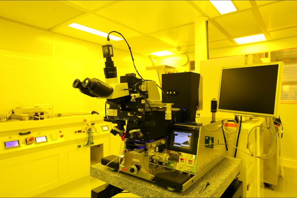
Plate 01Suss Microtech MJB4 Mask Aligner #62104
Bid ServicellcWatch on YouTubePlate 02Karl Suss MJB4 Mask Aligner Demonstration
ClassOneVideosWatch on YouTubePlate 03MJB4 Demo Video
Ollie Dunne Tara SemiWatch on YouTubePlate 04Süss MicroTec - MJB4
Virgin Lands - Technische VisualisierungWatch on YouTubePlate 05Suss Microtech MJB4 Mask Aligner #60960
Bid ServicellcWatch on YouTube
Wafer size
100mm
Node / era
about 800 nm
Vacuum
Soft, hard, and vacuum contact[2]
Performance
Top side alignment (TSA)[1]
Optics
Mercury (Hg) lamp[1]
What it is
Mask aligners are exposure tools used in photolithography to transfer patterns from a mask onto a photosensitive-coated substrate. The SUSS MicroTec MJB4 is a manual mask aligner designed for research and development environments. The MJB4 handles wafers and substrates up to 100 mm in diameter.[1][2]
How it works
Mask aligners expose substrates through a photomask using ultraviolet (UV) light. The MJB4 uses a mercury (Hg) lamp as its UV source, with spectral lines at 365 nm, 405 nm, and 436 nm. The default illumination setup provides 20 mW/cm² at 365 nm with an i-line filter installed, meaning only the 365 nm line is used for exposure.[1]
The MJB4 achieves parallelism between wafer and mask through a semi-automatic Wedge Error Compensation (WEC) procedure. Alignment is performed manually with micrometer knobs, offering an alignment precision of about 0.5 µm. The system supports top-side alignment (TSA) using a split-field microscope mode. Some configurations also offer infrared alignment capability.[1][2]
What can it run?
Process applications and technology nodes documented for this tool.
- LED lithography
- MEMS
What do the numbers mean?
Vacuum & pumping4
- Contact and alignment features
- Wedge Error Compensation (WEC); splitfield mode; top side and infrared alignment; vacuum contact; universal optics option for UV 250, UV 350, and UV 400[2]
Wafer handling13
- Small wafer/chip handling
- Special offset objectives for alignment of small wafer/chips; minimum separation is 10 mm[1]
Optics & imaging35
Performance9
Configuration & options12
What does it need to run?
Site utility requirements, footprint, and infrastructure needed to install and operate this tool. Sourced from public records.
- Contact optionsSoft, hard, and vacuum contact[2]
- Mask holdersThree different holders with vacuum clamping[1]
- Contact modesSoft, hard, vacuum contact[2]
- Contact and alignment featuresWedge Error Compensation (WEC); splitfield mode; top side and infrared alignment; vacuum contact; universal optics option for UV 250, UV 350, and UV 400[2]
Where are the manuals?
Publicly hosted documents referencing this tool, linked at their original location. Hosted by the linked institutions — availability may change.
- User ManualManualepfl.ch
Generated from public-source data on file. Enter your email to access — nothing is published; details are routed privately.
Not publicly documented
Field notes
No research found yet — worked with this tool? Share what you know.
Frequently asked questions
What is the maximum substrate size the MJB4 can handle?
The MJB4 can handle wafers and substrates up to 100 mm (4 inch) in diameter.[1][2]
What is the alignment accuracy of the MJB4?
The manual micrometer knobs provide an alignment precision of about 0.5 µm.[1]
What type of light source does the MJB4 use?
The MJB4 uses a mercury (Hg) lamp with spectral lines at 365 nm, 405 nm, and 436 nm. The default setup has an i-line filter installed, delivering 20 mW/cm² at 365 nm.[1]
Not publicly documented
The following facts about the MJB4 are absent from this record as of this revision. First-hand knowledge or a citation closes a gap; every submission is reviewed before publication.
No publicly documented production dates or lifecycle milestones (introduction, end of production, EOL) for the MJB4 are on record.
Answerable by: OEM historical records or a trade-press announcement
No publicly documented variants, configuration options, or revision breakpoints of the MJB4 are on record.
Answerable by: an OEM product catalog or an engineer who ordered or specified the tool
The control-system platform and OS era of the MJB4 are not on record.
Answerable by: an engineer who operated it or OEM installation records
No publicly documented failure modes or field errata for the MJB4 are on record.
Answerable by: a field service engineer, process engineer, or maintenance technician
No publicly documented compatible parts, consumables, or accessories for the MJB4 are on record.
Answerable by: an OEM parts catalog or a service engineer
No research found yet — worked with this tool? Share what you know.
Sources & citations
Sources (5)Every fact above is drawn from these public sources
- [1]epfl.ch — epfl.chepfl.ch
- [2]pnf.uchicago.edu — pnf.uchicago.edupnf.uchicago.edu
- [3]Equipment Resources | CNF — cnf.cornell.educnf.cornell.edu
- [4]Tool Details - Harvard CNS — cns1.rc.fas.harvard.educns1.rc.fas.harvard.edu
- [5]苏斯贸易(上海)有限公司: MJB4: SUSS MicroTec — suss.com (Dec 1, 2010)web.archive.org
Last updated Oct 8, 2026.
Compare with similar tools
View all →ASML PAS 5500/300 is a deep-UV stepper photolithography tool configured for 4-inch wafers.

The GCA 6100 C Wafer Stepper is a lithography tool for 100 mm wafers with a 150 mm X/Y stage travel and an AWH1 automatic wafer handler.
The OAI 808 Aligner is a semi-automated, four-camera, optical front- and backside mask aligner with stated alignment accuracy of 1µm to 2µm.
The OAI Model 800 Mask Aligner is a semi-automated, four-camera, optical front- and backside mask aligner with motorized backside focus, motorized auto leveling, and auto gap setting.
